S2C Dual VU440 Prodigy™ Logic Module
The Dual VU440 Prodigy Logic Module is S2C’s 6th generation SoC/ASIC prototyping system based on Xilinx’s Virtex UltraScale XCVU440 FPGA. The system has 1,200 general purpose I/Os and 64 GTH transceivers on 12 high-speed connectors, and users have access to S2C’s 80+ daughter cards to quickly build prototype targets. In addition, users can perform an array of runtime features remotely through both Ethernet and USB. Up to 16 Dual VU Logic Modules can be configured in a Cloud Cube™ to support a large-scale SoC/ASIC and to be shared among multiple users.
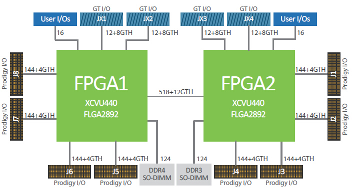
I/O Architecture
Features
Large Capacity & Scalable
- 11.08M System Logic Cells and 177.2 Mb of internal memory
- On-board DDR4 SO-DIMM socket and DDR3 SO-DIMM socket support up to a total of 16GB of memory
- Multiple Logic Modules can be conveniently connected together to expand capacity through interconnection modules or cables
- Up to 16 Dual VU Prodigy Logic Modules can be configured in a Prodigy Cloud Cube
High Reliability
- Screw-lock design to I/O connectors
- Self-Tests – Isolate design issues from board issues conveniently with a software GUI
- Monitoring of on-board voltage, current and temperature with a software GUI
- Automatic shut-down upon detection of over-current, over-voltage or over-temperature
Advanced Clock Management
Standalone Mode
- 6 global clocks to be selected from
– 6 programmable clock sources (0.2-700MHz)
– 5 pairs of external clocks through MMCX connectors
– 1 OSC socket - 3 feedback clock lines for internally generated clocks from any of the two user FPGAs
- 3 design clock outputs
– through 3 pairs of MMCX connectors
Cloud Cube Mode
- 6 global clocks to be selected from
– 6 local programmable clock sources (0.2-700MHz)
– 6 Cloud Cube global clock resources - 3 feedback clocks
– Internally generated clocks in any FPGA can be output to Cloud Cube global clock sources
High Performance
- Up to 100W of power for each FPGA
- Equal trace length for I/Os from same I/O connector
- On-board support of high-speed DDR3 and DDR4 memory
Flexible & Powerful I/Os
- 1,152 general purpose I/O pins and 32 GTH transceivers on 8 Prodigy Connectors
- Prodigy Connector I/O voltage on can be adjusted to 1.2V, 1.35V, 1.5V or 1.8V through runtime software in GUI with 4 status LEDs on-board to indicate I/O voltage
- 32 GTH transceivers and 48 general purpose I/O pins for control signals on 4 GT connectors
Pin-Multiplexing Interconnection Support
- 518 physical interconnections between the 2 FPGAs optimized for pin-multiplexing using LVDS
- Support for 30000+ design interconnections between two FPGAs with LVDS running at 1.2GHz
- Optional Prodigy Player Pro™ Compile Software for automatic design partitioning and LVDS pin-multiplexing insertion
- 12 additional gigabit transceiver interconnections between the two FPGAs
Ease-of-Use
- Auto detection of daughter cards or cables
- On-board battery charging circuit makes FPGA bin file encryption easy
- Compatible with S2C’s off-the-shelf pre-tested daughter boards
- Multiple FPGA configuration options through Ethernet port, USB port, JTAG and micro SD card
- Virtual SWs & LEDs for simple tasks such as changing a setting or indicating a condition remotely
- Optional S2C design implementation software
- Optional S2C Prodigy Multi-Debug System for multi-FPGA deep-trace debug through gigabit transceivers
- Optional ProtoBridge™ AXI software to co-model with software/simulation models in transaction-level
Other news

.jpg)


