S2C Quad KU115 Prodigy™ Logic Module
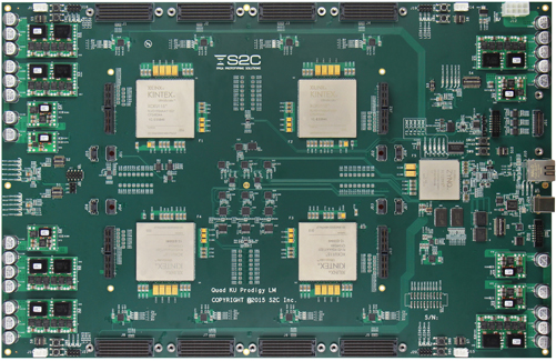
The Quad KU115 Logic Module is S2C’s 6th generation SoC/ASIC prototyping hardware that is populated with four Xilinx Kintex UltraScale XCKU115 FPGA devices. The Quad KU115 Logic Module is designed for massive parallel DSP calculation tasks with each KU115 device containing 5,520 DSP Slices. Large numbers of Quad KU115 Logic Modules can be formed in a MESH configuration to obtain the largest parallel DSP processing power in S2C’s Prodigy Cloud Cube™, an enterprise-class prototyping system. The Quad KU Logic Module provides access to 1,200 general purpose I/Os and 64 GTH transceivers on 12 high-speed connectors. Users also have access to S2C’s vast library of 80+ daughter cards to quickly build prototype targets.
I/O Architecture
Features and Benefits
Large Capacity & Scalable
- 5.8M System Logic Cells
- 303.6Mb of FPGA internal memory
- 22,080 DSP Slices
- Each Prodigy Connector can support 8GB of DDR3 or DDR4 memories through optional daughter cards
- Multiple Logic Modules can be conveniently connected together to expand capacity through the use of interconnection modules or cables
Flexible & Powerful I/Os
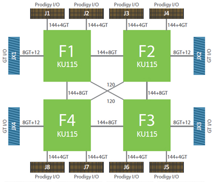
- 1,152 high-performance I/O pins and 32 Gigabit transceivers through 8 Prodigy connectors
- I/O voltage can be adjusted to 1.2V, 1.35V, 1.5V or 1.8V through runtime software in GUI with 4 status LEDs on-board to indicate I/O voltage
- 32 Gigabit transceivers and 48 GPIOs through 4 GT I/O connectors
Advanced Clock Management
Standalone Mode
- 6 global clocks to be selected from
– 6 programmable clock sources (0.2-700MHz)
– 5 pairs of external clocks through MMCX connectors
– 1 OSC socket - 3 design clock outputs
– through 3 pairs of MMCX connectors
Cloud Cube Mode
- 6 global clocks to be selected from
– 6 local programmable clock sources (0.2-700MHz)
– 6 Cloud Cube global clock resources - 3 feedback clocks
– Internally generated clocks can be output to Cloud Cube global clock sources
High Performance
- Up to 80W of power for an FPGA
- Equal trace length for I/Os from same I/O connector
High Reliability
- Screw-lock design to high-speed I/O connectors
- Self-Tests – Isolate design issues from board issues conveniently with a software GUI
- Monitoring of on-board voltage, current and temperature with a software GUI
- Automatic shut-down upon detection of overcurrent,over-voltage or over-temperature
Ease-of-Use
- Multiple FPGA configuration options through Ethernet port, USB port, JTAG and micro SD card
- Auto detection of daughter cards and cables
- Virtual SWs & LEDs for simple tasks such as changing a setting or indicating a condition remotely
- User Test Area – LEDs, Push Buttons, Switches and Pin Headers for testing and debugging
- On-board battery charging circuit makes FPGA bin file encryption easy
- Optional ProtoBridge™ AXI software to co-model with software/simulation models at the transaction-level
- Optional S2C design implementation & debug software
- Compatible with S2C’s off-the-shelf pre-tested daughter boards
Other news


