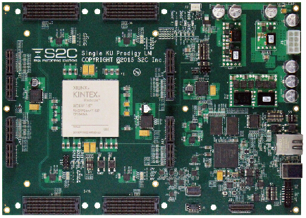
S2C Single KU115 Prodigy™ Logic Module
The Single KU115 Prodigy Logic Module, based on Xilinx’s Kintex UltraScale XCKU115 FPGA, is the ideal solution for today’s consumer-based Internet of Things (IoT) designs and other small to medium-sized SoCs. Prodigy KU is well-suited for calculation-intensive applications with 5,520 DSP slices, the most of any other solution on the market. The system has 656 general purpose I/Os and 48 GTH transceivers on 8 high-speed connectors enabling high-speed communications. This low cost, all-purpose, stand-alone prototyping system is integrated with S2C’s market-leading, vast library of daughter cards to quickly build prototype targets.
I/O Architecture
Features and Benefits
Large Capacity & Scalable
- 1.45M System Logic Cells
- 75.9 Mb of FPGA internal memory
- 5,520 DSP Slices
- Multiple Logic Modules can be conveniently connected together to expand capacity through the use of interconnection modules or cables
- Up to 16 Single KU Logic Modules can be configured in a Cloud Cube
High Reliability
- Screw-lock design to high-speed I/O connectors
- Self-Tests – Isolate design issues from board issues conveniently with a software GUI
- Monitoring of on-board voltage, current and temperature with a software GUI
- Automatic shut-down upon detection of overcurrent, over-voltage or over-temperature
Flexible & Powerful I/O
- 576 high-performance I/O pins and 16 Gigabit transceivers through 4 Prodigy connectors
- I/O voltage can be adjusted to 1.2V, 1.35V, 1.5V or 1.8V through runtime software in GUI with 4 status LEDs on-board to indicate I/O voltage
- 32 Gigabit transceivers and 80 GPIOs through 4 GT I/O connectors
High Performance
- Up to 80W of power for an FPGA
- Equal trace length for I/Os from same I/O connector
- 48 Gigabit Transceivers can run at 12.5Gbps
Advanced Clock Management
Standalone Mode
- 6 global clocks to be selected from
– 6 programmable clock sources (0.2-700MHz)
– 5 pairs of external clocks through MMCX connectors
– 1 OSC socket - 3 design clock outputs
– through 3 pairs of MMCX connectors
Cloud Cube Mode
- 6 global clocks to be selected from
– 6 local programmable clock sources (0.2-700MHz)
– 6 Cloud Cube global clock resources - 3 feedback clocks
– Internally generated clocks can be output to Cloud Cube global clock sources
Ease-of-Use
- Multiple FPGA configuration options through Ethernet port, USB port, JTAG and micro SD card
- Auto detection of daughter cards and cables
- Virtual SWs & LEDs for simple tasks such as changing a setting or indicating a condition remotely
- User Test Area – LEDs, Push Buttons, Switches and Pin Headers for testing and debugging
- On-board battery charging circuit makes FPGA bin file encryption easy
- Optional ProtoBridge™ AXI software to co-model with software/simulation models at the transaction-level
- Optional S2C design implementation & debug software
- Compatible with S2C’s off-the-shelf pre-tested daughter boards
Other news


